
What Is NAND Flash Memory? Definition, Types, and Uses

NAND flash memory is a type of non-volatile semiconductor memory that stores digital data without continuous power. It provides the storage inside SSDs, USB flash drives, SD cards, and many smartphones. NAND flash storage commonly refers to storage based on this technology.
NAND is the memory medium inside a device. A complete storage device also needs a controller and supporting software to organize access, communicate with the host system, and manage errors. That distinction explains why products using similar flash chips can deliver different performance and reliability.
Table of Contents
NAND Flash Memory at a Glance
Feature | Meaning |
Technology category | Non-volatile flash memory |
Storage mechanism | Electrical charge changes the states of memory cells |
Power requirement | Power is needed to read, program, and erase data, but not continuously to retain it |
Basic organization | Cells organized into pages and erase blocks |
Common cell types | SLC, MLC, TLC, and QLC |
Physical layouts | Planar NAND and vertically stacked 3D NAND |
Typical applications | SSDs, removable storage, mobile devices, and embedded systems |
Main limitations | Finite program/erase endurance and condition-dependent data retention |
NAND belongs to the wider family of flash memory technologies, which also includes NOR flash.
NAND Flash Storage Explained in Plain English
When a phone saves a photo, the image becomes digital data stored in flash cells. Those cells retain their stored states after the phone shuts down. When the photo is opened again, the storage system retrieves the data so the application can display it.
Several layers cooperate:
- The file system organizes filenames, folders, and information about where file contents are stored.
- The storage controller manages access to the physical memory.
- The NAND cells hold the underlying bits.
The cells do not understand a filename such as holiday.jpg. Filenames and folder information are themselves stored as data, which software interprets.
In everyday usage, NAND flash memory and NAND flash storage often describe the same underlying technology. More precisely, memory refers to the semiconductor medium, while storage can describe the complete implementation built around it.
How NAND Flash Memory Works
Three operations explain the basic mechanism: reading, programming, and erasing. Programming is the technical term for writing data into flash cells.
Electrical Charge Represents Data
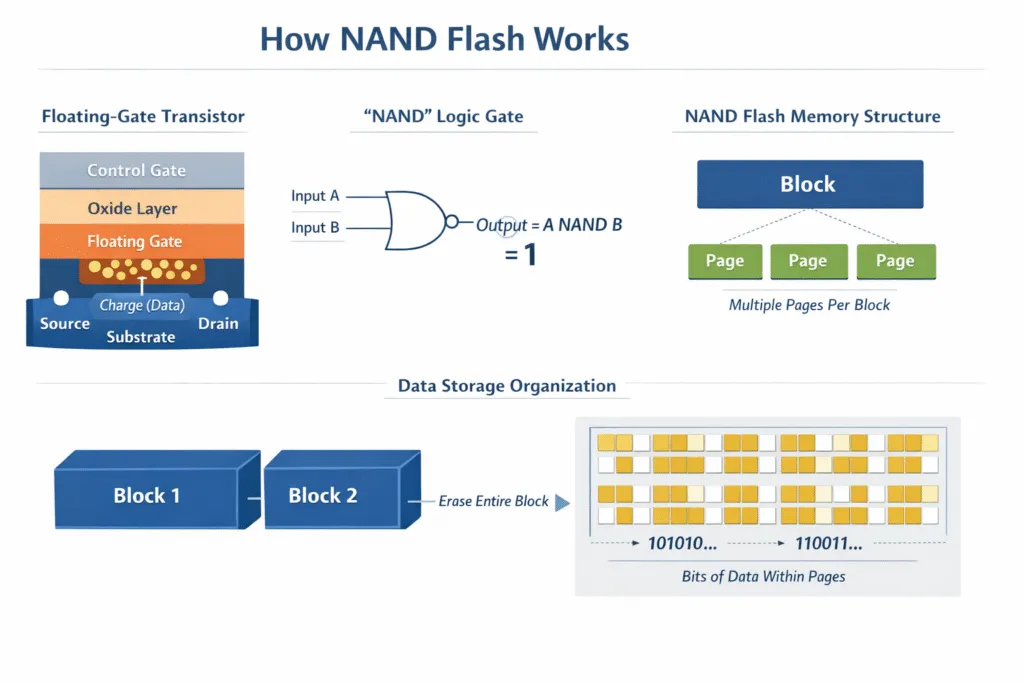
A NAND cell stores information through electrical charge that changes its threshold voltage—the voltage needed to make its transistor conduct.
Read circuitry distinguishes between voltage ranges and interprets them as digital values. A one-bit cell needs two distinguishable states. Cells that store multiple bits need additional states.
NAND designs use different charge-storage structures, including floating gates and charge traps. Consequently, describing all NAND as floating-gate memory is too restrictive. KIOXIA’s technical brief on NAND endurance discusses the use of charge-trap technology in 3D NAND.
Pages Are Programmed and Blocks Are Erased
NAND operations work at different levels:
Unit | Role |
Cell | Holds an electrical state representing one or more bits |
Page | A unit used for reading and programming data |
Block | A group of pages erased together |
Exact page sizes, block sizes, and programming restrictions depend on the chip. A physical NAND page is different from a file-system allocation unit or a logical sector exposed to the operating system.
The central constraint is that previously programmed space cannot be freely overwritten like ordinary RAM. A block must be erased before its programmed pages can be reused. Kingston’s explanation of garbage collection describes this difference between page-level writes and block-level erasure.
Updating Data Usually Means Writing Elsewhere
Suppose part of a document is stored in Page A. When that part changes, a managed flash device typically writes the updated content into an available Page B and changes its address mapping to point there.
Page A then contains an outdated copy. Marking it invalid does not immediately erase the block containing it.
Stage | What happens | Result |
Before the update | The mapping points to Page A | Reads return the original data |
Write the update | Updated data is programmed into Page B | The new version has a separate physical location |
Change the mapping | The mapping points to Page B | Future reads retrieve the updated version |
Invalidate the old copy | Page A is no longer needed | Its space can be reclaimed later |
Reclaim the block | Remaining valid pages are moved before the old block is erased | The erased block becomes available for reuse |
This is a simplified example of a data update, rather than a claim that an entire document always fits into one page.
The later reclamation process is called garbage collection. It preserves data that is still needed, then erases the selected block. KIOXIA’s garbage collection technical brief explains the separation, relocation, and erasure stages.
Moving valid data creates additional internal writes. This contributes to write amplification, where the flash receives more writes than the host originally requested. It is one reason workload and internal management affect endurance.
Management Keeps the Memory Usable
NAND flash memory needs management functions around its physical cells:
- Error correction detects and corrects errors within the system’s capability.
- Bad block management avoids blocks that cannot reliably store data.
- Wear leveling distributes program/erase activity instead of repeatedly wearing the same locations.
With raw NAND, the host supplies much of this management. Managed flash integrates a controller to handle these responsibilities, although intermediate designs also exist. Micron’s guide to choosing NAND explains these distinctions.
Types of NAND Flash Memory
Two classifications matter most: how many bits each cell stores and how the cells are physically arranged. These describe different properties.
SLC, MLC, TLC, and QLC
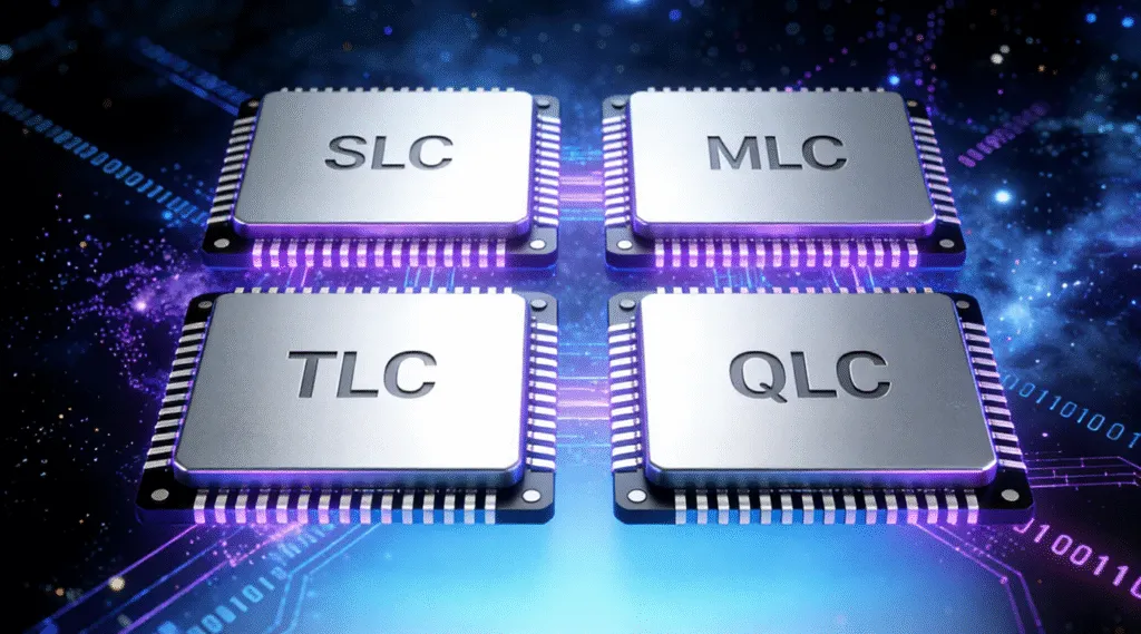
Storing more bits in each cell increases density. It also requires the device to distinguish more electrical states.
Type | Full name | Bits per cell | Required states |
SLC | Single-Level Cell | 1 | 2 |
MLC | Multi-Level Cell | 2 | 4 |
TLC | Triple-Level Cell | 3 | 8 |
QLC | Quad-Level Cell | 4 | 16 |
In conventional product terminology, MLC normally means two bits per cell, although “multi-level” can have a broader technical meaning.
For comparable designs, fewer bits per cell generally provide greater endurance and simpler programming. More bits increase density and can reduce cost per gigabyte. KIOXIA’s overview of NAND endurance explains these trade-offs.
These labels do not establish a complete device’s speed or lifespan. Controller design, firmware, available capacity, interface, and workload also matter. A universal endurance figure for every TLC or QLC product would therefore be misleading.
Planar NAND and 3D NAND
Planar NAND arranges cells across a two-dimensional surface. 3D NAND stacks cells vertically, increasing storage density within a given footprint.
The two classifications can be combined. A chip described as 3D TLC NAND uses a vertically stacked layout and stores three bits per cell. Similarly, 3D QLC stores four bits per cell.
Micron’s overview of flash technology explains how vertical stacking increases capacity without a proportionally larger chip footprint.
Benefits and Limitations of NAND Flash Storage
The characteristics that make NAND useful also explain its limitations.
Compact Storage Without Moving Parts
NAND stores data electronically, allowing substantial capacity in small packages. It does not require spinning platters or a moving read/write head.
This supports compact, silent storage and resistance to mechanical shock. NAND-based devices can also provide low access latency and suit battery-powered equipment.
However, no moving parts does not mean no failure points. Connectors, controllers, supporting electronics, and memory cells can still fail. Actual speed and power consumption depend on the complete device.
Finite Program/Erase Endurance
Programming and erasing stress flash cells. Accumulated wear makes their stored states harder to distinguish reliably.
There is no single program/erase rating for all NAND flash memory. The rating depends on the technology, manufacturing generation, operating conditions, and specified reliability requirements.
Finished SSDs commonly use device-level endurance ratings such as terabytes written, or TBW. TBW describes a specified write volume for the drive; it is different from a program/erase cycle rating for the underlying NAND.
Data Retention Is Finite
Non-volatile means that continuous power is unnecessary to retain data. It does not guarantee that data remains readable indefinitely.
Stored charge can change over time. Previous wear, temperature, and electrical interference affect reliability. Error correction compensates within its designed limits, but cannot guarantee recovery from every error. Research on flash memory errors and mitigation examines these mechanisms.
For important information, keeping another verified copy matters more than assuming an unplugged flash device will preserve it forever.
Performance Depends on the Complete System
NAND type is one influence on performance. The controller, interface, firmware, and workload also affect the speed users experience.
For example, a sustained write workload may require garbage collection and data relocation. The amount of internal work depends partly on how much reusable space is available.
A product’s use of NAND therefore does not establish a particular transfer rate. Micron identifies the controller, NAND type, and host interface as factors affecting storage performance.
NAND Flash Compared with Related Technologies
The most useful comparisons separate the memory medium from the device or interface built around it.
Comparison | Main distinction | Practical meaning |
NAND vs NOR flash | Different flash architectures and access characteristics | NAND suits dense data storage; NOR suits uses such as firmware and direct code access |
NAND vs system RAM | Persistent storage versus volatile working memory | Ordinary DRAM loses its contents without power; NAND retains stored data |
NAND vs SSD | Memory medium versus complete storage device | A typical SSD contains NAND, a controller, firmware, and a host interface |
NAND vs HDD | Semiconductor storage versus magnetic storage | Both retain data without power, but use different physical mechanisms |
NAND vs eMMC or UFS | Memory medium versus managed storage technologies | eMMC and UFS products incorporate NAND, management functions, and a defined host interface |
NOR’s access characteristics are useful for reading small amounts of data and supporting code execution. NAND’s organization favors high-density storage. Neither is universally better: their suitability depends on the system’s requirements. Kingston’s Flash Memory Guide explains their access differences.
Likewise, “NAND or SSD?” compares different layers. NAND is the storage medium used inside a typical SSD.
Where You Encounter NAND Flash Memory
Common applications include:
- SSDs: operating systems, applications, and user files.
- USB flash drives: removable storage accessed through USB.
- SD and microSD cards: storage for cameras and other compatible devices.
- Smartphones and tablets: internal storage, often using managed flash.
- Embedded equipment: storage in networking, automotive, and industrial systems.
Users normally encounter these device categories rather than the individual NAND chips.
How to Read a NAND Specification
Consider a product described as “1 TB SSD with 3D TLC NAND.”
Specification | What it tells you | What it does not establish |
1 TB | Advertised storage capacity | Write endurance or access speed |
SSD | The category of storage device | Its precise NAND architecture |
3D | Cells use a vertically stacked layout | Bits stored per cell |
TLC | Each cell stores three bits | The finished drive’s exact performance or lifespan |
To identify the NAND in a particular device, check documentation for the exact model and hardware revision. A drive letter, partition format, or file-system name cannot identify its cell type.
For controller behavior and other device-level details, see the separate SSD NAND flash memory guide.
Common Misconceptions About NAND
“Non-Volatile Means Permanent”
It means stored data can survive power removal. It does not guarantee unlimited retention, protection against deletion, or survival after hardware failure.
“Every File Update Erases an Entire Block Immediately”
Managed flash normally writes updated data elsewhere and changes its mapping. Block erasure takes place when space is reclaimed. Confusing these stages makes both performance and endurance harder to understand.
“Deleting a File Immediately Erases Its NAND Cells”
File deletion, logical address deallocation, and physical erasure are different operations.
On supported storage paths, TRIM or a similar command tells the device that certain logical ranges are no longer needed. The device then handles those ranges according to its implementation.
Even if physical erasure has not yet occurred, the original data may no longer be readable through the normal interface. Microsoft’s TRIM documentation explains that subsequent reads may return original data, zeros, ones, or a combination.
“Recovery Software Reads the Chips Directly”
Ordinary file-recovery software reads storage exposed through the operating system and device interface. It does not directly probe individual NAND cells or bypass a failed controller.
A deeper scan cannot reconstruct original content from ranges that no longer expose that content. Physical charge remaining somewhere inside a chip does not, by itself, establish software recoverability.
When Further Action Is Needed
Understanding NAND flash storage helps interpret specifications and recognize the limits of a device. Routine use does not require manually managing its pages or erase blocks.
If files disappear, avoid writing new data or reformatting the affected device before assessing the situation. Recovery depends on the remaining readable data and the failure involved.
For missing files on camera storage, the SD card recovery guide provides the relevant next steps. A device that repeatedly disconnects or cannot be read may require hardware assessment rather than repeated software scans.
Conclusion
NAND flash memory stores information as electrical states that persist without continuous power. Its page-based programming, block-based erasure, and compact cell structures support a wide range of storage devices.
Distinguishing the cells from the controller and finished device makes specifications easier to understand. It also explains why fast, non-volatile storage still has limits involving wear, retention, and data availability.
FAQ
What does NAND stand for?
Is NAND flash storage the same as NAND flash memory?
Does NAND flash need a battery to retain data?
Does reading NAND flash wear it out?
Can formatting repair worn-out NAND cells?
Can NAND flash replace a computer’s RAM?
Why does a device show less usable capacity than its NAND capacity?
Does a corrupted file mean the NAND chips are damaged?

Vasilii is a data recovery specialist with around 10 years of hands-on experience in the field. Throughout his career, he has successfully solved thousands of complex cases involving deleted files, formatted drives, lost partitions, and RAW file systems. His expertise covers both manual recovery methods using professional tools like hex editors and advanced automated solutions with recovery software. Vasilii's mission is to make reliable data recovery knowledge accessible to both IT professionals and everyday users, helping them safeguard their valuable digital assets.